Transcription from scanned papers - originally called 'KS Repair Guide'
|
01. Address clock 02. Multiplexers 03. Touch Sensitivity 04. D type Short Term Memory 05. Random Function 06. DAC 07. Dynamic Response 08. Record And Play Touch Pads + Memory Control Logic 09. Shift Register Memory + Gates 10. Shift Register Memory + Clock Generator - Skipshift 11. Meter DAC + Clock Generator - Skip and Shift 12. Memory DAC 13. Transposition Pads 14. Appendix 15. Functional Diagram extra : 16. TTL pinouts |

|
| Shift Register : MF50052T or MF7104 | |
|
FIRSTLY. The Touch Keyboard and address clock.
The address clock is an oscillator, E28 (Pins 1,2,4,5,6), being a conventional schmitt trigger oscillator. OPERATION Pin 6 is high; D38, 43 are off, C1 and C1x charged up by way of Pins 1,2,4,5 until upper threshold voltage (about + 1.7v) is reached, the schmitt trigger then fires, Pin 6 goes low, D38, 43 turn on and discharges C1 and C1x until the lower threshold voltage (about 0.9v) is reached. The schmitt then reverts back to its original state etc.etc. |

|
|
The pulse generated are used to compile various gating signals. The signal is divided by 2 by E22 (8,9,11,12) and again by E22 (2,3,5,6), and then by 16 by E23. By gating these signals together, a set of waveforms shown below is produced. |

|
|
SIGNALS A1, A0, B0, C0 provide a four bit address code to the three data multiplexers. The top two multiplexers, E15, E27 are connected to the keyboard, and as only 30 notes are provided, then two inputs (E27 plus 7,8 are left ?? ...(text outside scan) |
| MULTIPLEXERS - an electronic 16 way switch; single pole. |

|
| The 16 inputs, E0 to E15, can be considered as the 16 inputs to a rotary switch. The switch position (only one pole) is determined by the address code, ie A0,A1,B1,C1, labelled ABCD on the actual device. |

|
|
The ENABLE SIGNAL acts as a switch; that is when this signal is high (1) the switch is open circuit, and the output (w) is permanently high. When this signal is low (o) the switch is closed and so anyone of the 16 data inputs may be selected. The 'ENABLE' IS SOMETIMES called the STROBE. Note that the output shows the inverted data. Thus to summarise. With a high (1) at data input 12, and address code of A=1, B=1, C=0, D=1 and an enable signal of logic 0, the output is (1) inverted, namely 0. |
|
TOUCH SENSITIVITY. The input to a TTL gate looks like : | |

|
This is a multiple emitter transistor, i.e. a transistor with, in this case, 6 emitters. |
|
In the multiplexer, 4 of them are connected to the address code, one to the enable signal and the last to the touch plate. | |

| |
|
For each specific input there will only be one point in the Address cycle (32 bits) when all 5 emitters are high at the same time. When the bias is correctly aligned, the circuit will behave as follows : | |

|
looking at the last trace we see that sixth emitter, which is connected to the touch plate, is dragged up, due to the associated capacitance of itself WRT its sister emitters. in this case, 6 emitters. |
|
Infact, it is dragged up so far that it changes state from a '0' to a '1'. BUT when a finger is placed on the associated touch plate, the capacitance of the finger increases the total capacitance as seen by the emitter, increasing it by as much as 10 to 100 pF, and this is sufficient to prevent it from changing state. | |

|
Thus, pressing the pad with a finger will prevent the data multiplexer output from changing state |
| The enable signals 'M' and 'N' are | |

|
Thus one multiplexer is addressed, and then the other (i.e. E15 and 27) is then the other etc. |
|
If more than one note is pressed, then several gaps in the outputs will be generated; however; the electronics that follow select the first note to appear, and as the keyboard is swept (addressed) from top to bottom, then the highest note pressed is selected. This piece of electronics is E26 (11,12,13) (4,5,6) E25 (8,9,10,11,12,13), E16, E17, E18. The two data inputs of MULTIPLEXERS E15, E17 are OR'ED together by E26 (11,12,13) (that is they are effectively just added together). | |

| |
| * WHEN looking for these waveforms, you much SYNC OFF of D0 E23/11. | |
|
Now consider the 'D' type E25 (8,9,10,11,12,13). Assume that pin 8 is at logic 1. Therefore, Pin 5 E26 is at logic 1, and it is thus "enabled" in that it allows signals at its other pin (pin 4) to pass through it. The signal at pin 4 is the summed data output, which when it passes through the gate, is inverted. Notice that the clock pulses are coherent with the data signal. | |

|
The D type operate as follows. It is an edge triggered device; that is data at its' D input is transferred to the Q output on the +ve transition of the clock. |
|
That is, put a 1 on pin 12, clock the device and a 1 appears at pin 9, the Q output. So, in the present example, when there are no notes pressed, the data is low when it is clocked, and so Q remains Low. But, when that data is high, then Q goes high, therefore Q (pin 8) goes low and in doing so inhibite E26 (4,5,6) the output of which thus remains high. The circuit has latched up, and it will remain latched up until it is released by a clearing pulse. | |

|
Thus, E25, Q9 goes high and remains there when it detects the first note. (See page 2, waveforms). Now, E25, Q9 clocks the D types E16,17,18, which are fed with the address code (A, Ao, Bo, Do,). So, as soon as the first note is detected, its address is clocked into E16,17,18 which act as a one bit memory. |
|
At the end of one address sweep (about 100 µsec.) the D type E25 is unlatched by a negative going pulse produced by differentiating the address bit Do (23 pin 11) with the CR network C4, R44 . | |
|
| |
|
A low on the clear input of a D type clears the Q output to logic 0. Thus, the D types E16, 17, 18 form a short term memory that is continually being updated (every 100 µsec) as to highest key that is being selected. The output Pin 9 E25 is an excellent place to test the keyboard to see if the multiplexer for the KB and/or the address code is functioning. | |

|
2nd bottom note pressed. |

|
As you sweep your finger up the keyboard the waveform changes as shown. (The pulse width elongates) |
|
RANDOM FUNCTION This is the same touch sensitive detector as for the KEYBOARD. However, as there is only one input, then no addressing is required. | |

|
A slow clock pulse generator is used, (5KHz, 60 nsec. pulses). A separate oscillator, rather than the address oscillator is used, because : 1. A long enough gap must be provided to allow the floating gate time to discharge. 2. If the address clock were to be used, the Random would not be random; this is because the network has a tendency to select the largest clock pulse and this means that particular notes occur more readily than others. |
|
The operation is as follows. When a missing pulse is detected by E25 pin 2, the ¬Q output goes low and so the cct folds over. The ¬Q is connected to the set input of E25. This will cause the Q output to go high and in doing so it 'records' an address. ( Any address in fact; it depends upon when the Random is pressed ). When the random is released, the set input of E25 pin 10 returns to 1, and the circuit operates as before. As the Q output E25 pin 6 can go low at any point in time, then any note is selected, and hence the term 'random'. N.B. The random function can generate errors; this is a design error. The errors can be generated by the random accidentally selecting address code Binary 11111 (i.e. 32). This is the 'Skip' code, and it will cause the meter to prematurely reset, and the memory to corrupt. To demonstrate this phenomenon, try this test : Set the Sequencerb clock speed to about 3 to 4 on the knob, press record and then tap the random pad. There is a 32:1 chance of generating the skip code, and this will be detected by a premature reset of the meter. | |
|
DAC The short term memory E16,17,18 feeds Q1 to 5 which form a DAC ( Digital to Analogue Converter ) Slightly re-drawing the circuit, we the following : | |

|
Inside the dotted box are 5 resistors and 5 switches. The resistors are R49 to R54, 1% m.o. resistors. The switches are Q1 to 5 and these are controlled by the stored address in E16, 17, 18. When the address is 00000, all the switches are off, and so the circuit is just a simple differential amplifier, and the voltage at the output of A1 is 0V. When the switches turn 'ON', the output goes negative. |

| |
|
* NOTE WRT the short term memory E16,17,18. The lower half of E18 is different to the other 5 sections. This is the "key-pressed" section. It uses the clock line as its data input. This is because, when Q9, E25 is high, then a key is being pressed, and this is the data ir requires. It is clocked by ¬Do (known as ¬F@8, E26) at the end of an address sweep, and so its Q output (i.e. 9, E18) is high, when a key is pressed and low when no key is pressed. Note that the negative (1-0) transition of the ¬Q output (8, E16) is used to control the envelope trigger by turning transistor Q6 on when a key is pressed. The envelope trigger control pot is used to determine whether the trigger is generated from the real time or recorded output. | |
|
DYNAMIC RESPONSE The crystal gives the K.B. a dynamic function, but this is only employable in real time. That is, no information about the key pressure is recorded. The crystal produces a click when the K.B. is hit. | |

|
The network is a voltage follower with a diode in the feedback loop. The junction between the diode and the capacitor tries to follow the +ve voltage transient of the input and decays slowly (due to the storage of the capacitor) after the signal has ceased. |
| This voltage is used to control one of the output channels on a Synthi A. | |
|
RECORD, PLAY, CONTROL * note Record and Play are clocked from the random clock gen. The RECORD and PLAY pads operate in the same way as the Random touch pad. However, the interconnection of E10 (1,2,3,4,5) with E10 (8,9,10,11,12,13) and E10 with E18, provide a sequential mode of operation. That is : | |

|
these two sequences are permissible. |

|
Nothing happens |

| |
|
1. The record pad is pressed. The data presented at the D input (2, E10) is high during the clock. Therefore Q goes high, ¬Q goes low. This sets E10 (* a low on its set input) and so the D type is latched up, and it will remain there until it is cleared. The ¬Q pin 6 is also connected to the clear of the lower E10 D type, but this has no effect as the D type is already in its cleared mode. 2. When the keyboard is pressed the KEY ↘ voltage (i.e. E18, 8) goes low, and this clears E10 (2,3.4.5.6). (the clear overrides the set control). The ¬Q output (E10, 6) then goes high, whereas the lower D type still remains unchanged. 3. Play is pressed. A logic high is presented to the D input (12, E10) and so the ¬Q goes low. However as there is no... 3a. latch up it returns to its high level as soon as the finger is released. Note, that when at the record mode, the clear input (13, E10) is low and so the lower half of E10 is prevented from changing state; that is, Record Play does nothing. | |
|
Control Logic This is E6. The logic sequence (Above ) is presented to E6. The output sequence generated by E6 is as follows : | |

| |

| |
|
Lines A and B open and close the sets of input/output gates. Only one set of gates (A or B) is ever open. When the logic level on A is high, gates connected to it are open. When the logic level on A is low, gates connected to it are closed. Record Mode : Both sets of gates are closed. Clock to shift registers is very fast, latter filled with 0's Keyb'd Mode. This is "record" mode (confused?); data is accepted, because A is high. The data is clocked into the shift register at a slower rate, this rate being variable. If you are unlucky, you can overfill the shift register, and the front of the data is merely lost out of the end of the device. Play. Data is replayed and recirculated, because line B is high. The replay clock rate is also variable. When an unfilled part of the shift register is detected a skip mode is implemented and the shift register skips all the blank locations until it finds the start of the data, which it then plays at its slow rate. Pressing the Play pad stops the shift clock from operating in its "play" mode and so pressing play whilst the machine is replaying does two things : 1. Effectively pauses the device. 2. Upon releasing finger, the sequence restarts (proceeded by a skip block). If the shift register has been overfilled, then there are no blank locations and so when the play is pressed, the machine rapidly searches for an empty location and cannot find one. The result is a buzz sound as all the data rapidly recirculates. Also, as there are no blank locations, the machine does not know where the sequence start is. Therefore overfilled sequences, when replayed will start anywhere. The memory is a 6 bit word, 256 bits long. 5 bits are used to record the note selected. The sixth is used to trigger the envelope trigger; that is if the envelope trigger pot is in the right position. |
|
SHIFT CLOCK/SKIP GENERATOR E19, Q14, C6, R71, R70, R72, VR3 is the high speed skip generator. It is a schmitt trigger oscillator. When C7 is operational the oscillator reverts to a low speed clock generator. In normal operation pin 8, E3 is low, C7 is thus effective and so a slow clock is generated. (Normal operation is during the recording and playing back, and not the pressing of those pads). In normal operation, the output of E2 is high (i.e. the input is not all 1's) and so is the input pin 9, E3. When RECORD is pressed, all the inputs to E2 are high, the output of E2 goes low, and sets the skip oscillator into its skip mode, by making C7 ineffective. The shiftregister is thus filled with 0's. Also, the two meterdivider circuits E20, E24 are reset to zero. When the KEYBOARD is pressed, the input gates to the shift registers are opened, and so the inputs to E2 change from all 1's to a mixture of 0's and 1's. (Note an all 1's condition cannot occur in normal operation). The output of E2 goes to 1. Thus the output pin 8 of E3 goes to 0, C7 is functional so the oscillator begins to clock in its slow mode. Also, the reset on E24, 20 is in its count mode, the clock being taken from E19 pin 8. | |

|
The output from E19, 8 is differentiated by C16, R68 to give a very sharp pulse, which appears at Q13's collector, and is used to drive all the shift registers. |

| |
|
When the PLAY pad is pressed. Input pin 9, E3 goes low (but only for the duration of the pressing of the pad); this causes the data to rapidly recirculate (skip), usually for one bit only (because E3, 8 is high). E3, 9 is low. Hence E19, 6 is high. E2, 8 is high. Nothing happens until an "all low-state" of the shift registers is detected by E2 (* all 1's as seen by E2). When this state is located, E2, 8 falls to 0, therefore E3, 6 goes high, and in doing so resets E20, E24. Also, there are now two high's at the input to E3, (1,2,3) and so E3, 3 goes low and in doing so disables E19 (8,9,10,11,12,13) the oscillator. If there are no empty storage locations, the network just rapidly recirculates, and a "buzz" is heard. When the play pad is released, pin 9, E3 goes high, however E3, 8 still remains high; E19, 6 takes a short time to go low because of the effect of C17. (This eliminates spurious effects when operating the play pad.) When E19, 6 goes low, E3, 3 goes high, thus enabling the clock oscillator. The clock is in its high speed mode (skip) and so it races past all the unused storage area and when it comes to the first piece of data, E2, 8 goes high, the clock thus reverts to its slow speed mode, and E24, E20 is set to its count mode. Thus the stored data is replayed, and when the end is reached there is a rapid skip and the process repeats itself. | |
|
METER COUNTER The clock is divided by +16 twice, which is 256, the length of the memory. THe 5 most significant bits are decoded in the meter DAC. This is E24 and the resistor network. The network is a "weighted/ladder" - (a Cockeral special). | |

| |

|
|
MEMORY DAC The second DAC is a 5 bit device with a 6th bit controlled by the transposition pad. The "transposition pad" bit is the same order of magnitude as the MSB of the address bits. |
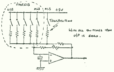
|
|
The switches are transistors Q7 and Q8--Q12 and the operation is similar to the real time DAC. Note, that the transposition acts only on the recorded output DAC, but no record of transposition playing is stored in the memory. Transposition is real time only. | |
|
TRANSPOSITION. The transposition multiplexer operates in a similar manner to the two other multiplexers. One difference is a feed-back circuit E11 (8,11,12) that causes single events to be multiplied. Looking at E7, we have : | |
|
|
The multiplexer is addressed in the usual way, and is enabled and has the same touch sensitivity as before. |
| When Eo is pressed, it is prevented from going high, and so the output at W is high for Eo. | |
| therefore pressing Eo produces a 1 bit pulse at E11 pin 8. |
|
|
Pressing the tone causes W to be high for E1. But the output ¬Q of E11 is fed back to E2. And so when E2 is addressed the output is again high but stops when it gets to E3 | |
| * Notice E14, E15 are never low. |
|
|
Now, the output from E11 pin 8 is used to control the DAC on the recorded output. As the transposition signal is a mark/space ratio signal, then the resultant product from the DAC must be smoothed out, this being accomplished by C5. THe transposition signal is used to control a logic switch of equal status to the MSB of the 5 bit DAC. The thirty notes available from the keyboard form 2½ octaves. (i.e. 12 notes per octave). Therefore 12 logic bit = 1 Octave or 1 semitone = 1 logic bit. where 1 octave = 12 semitones. The MSB of the address is equivalent to 16 logic bits. Therefore as the transpose controls a switch of equal status to the MSB, then one bit of the transpose signal = 1 semitone. Therefore, pressing the ½ tone pad = 1 bit = 1 semitone. pressing the tone pad = 2 bits = 2 semitones. pressing the third pad = 4 bits = 4 semitones. pressing the fifth pad = 7 bits = 7 semitones. that is, pressing the keyboard and the transposition-pad, transpose the note generated upwards by the respective amount. * Example : pressing the ½ tone, third and fifth will shift a note up by one octave. (That is, if the keyboard has been adjusted to 2½ octaves) 1 + 4 + 7 = 12 semitones = 1 octave. (* An octave - the ratio of two frequencies which are at frequencies of F and 2F. F being arbitary). | |
| APPENDIX | |

|
D type, used usually as a one bit delay or an edge detector. |
|
Logic data is presented to the D input. The data (0 or a 1) appears at the Q output after the +ve edge of the clock pulse, that is : data is transferred to the Q output on the +ve edge of the clock : Set - a 0 on the setputs Q to 1 Clear - a 0 on the clear puts Q to 0 set and clear are independant of the clock and override the D input. | |
| SCHMITT | |

|
The SN7413N looks like 4 input AND, followed by a schmitt trigger, followed by an inverter. |
|
The schmitt trigger exhibits a phenomena known as Hysterysis. |

|
| FUNCTIONAL DIAGRAM |

|
|
TTL Pinouts
7400 - Quad 2-Input NAND Gate 7403 - Quad 2-Input NAND Gates with Open-Collector Outputs 7404 - 6 Inverters 7410 - Triple 3-Input Positive-Nand Gates 7413 - Dual 4-Input Positive-Nand Schmitt Triggers 7474 - Dual D-Type Positive-Edge-Triggered Flip-Flops With Preset And Clear 7493 - Decade, Divide-By-Twelve And Binary Counters 74150 - Data Selectors/multiplexers |

|